HOT Search
Hot News

Product recommendation


In recent years, with the continued rise in popularity of outdoor leisure activities such as self-driving tours, camping, and picnics, the demand for "off-grid electricity" away from the power grid is experiencing explosive growth.
Whether it is electricity for induction cookers, kettles, and electronic products, or electricity for outdoor live streaming, outdoor work, and emergency rescue, users have put forward higher requirements for the power density, charging speed, and safety of portable energy storage power supplies (outdoor power supplies).

However, portable energy storage power supplies (outdoor power supplies) are not simply "large power banks". They contain both high-voltage power circuits and low-voltage control circuits, and can directly output 110 /220V high-voltage electricity through the AC output interface .
Therefore, in order to ensure the electrical safety of people and equipment and meet the relevant safety certification requirements, engineers usually integrate digital isolators into the system to build a safe and reliable electrical isolation system.
As shown in the diagram below, a portable energy storage power system typically consists of multiple functional modules, including energy conversion, energy storage, energy management, logic control, safety protection, and external communication.
In this system , the digital isolator is mainly responsible for building a reliable electrical isolation communication channel between the various functional modules, thereby reducing adverse interferences such as electrical noise, surges, and ground potential differences between different voltage domains.
This ensures that the control unit, power conversion unit, and battery management system can still have stable and accurate data transmission capabilities under complex environmental conditions.

A schematic diagram of a common electrical isolation scheme for a portable energy storage power system.
The isolation driver chip is mainly responsible for establishing an electrical isolation barrier between the low-voltage control side and the high-voltage power side to block severe electromagnetic interference such as common-mode transients (dv/dt), instantaneous ground potential jumps, and bus surges generated by the high-voltage power circuit.
At the same time, it amplifies the weak PWM control signal output by the MCU to provide a fast and sufficient charging and discharging current to the gate of the power transistor, thereby ensuring that the switching transistor is turned on/off precisely according to the preset timing.
The isolation sampling chip is mainly responsible for building an electrically isolated signal transmission channel between the high-voltage power side and the low-voltage control side, safely converting high-voltage physical quantities such as bus voltage and current into low-voltage differential signals that can be acquired by the MCU; at the same time, it blocks the interference of common-mode noise and high-voltage surges in the power circuit on the sampling accuracy, ensuring that the MCU obtains real and accurate voltage and current feedback information, providing reliable data for the closed-loop regulation and overvoltage and overcurrent protection of the system .
The isolation interface chip is mainly responsible for building an electrically isolated communication transmission channel between the internal MCU and the external communication bus.
It converts the logic level output by the MCU into a differential signal that conforms to the bus standard. At the same time, it isolates common-mode interference, surges and ground potential differences introduced by external cables, prevents surge voltage introduced by external communication lines from damaging the internal low-voltage circuits and ground potential differences from damaging the internal low-voltage circuits, and ensures safe and reliable bidirectional data interaction between the energy storage system and external devices such as the host computer, BMS slave or display screen.
It is worth mentioning that in portable energy storage power systems, the realization of functional requirements such as anti-interference of communication links, reliability of power transistor drive, and accuracy of analog sampling ultimately relies on a series of isolation chips with high isolation withstand voltage and high common-mode immunity.


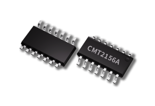
The CMT8602X is a series of isolated driver chips with 3.75/5.75kVrms isolation withstand voltage, CMTI≥±150kV/μs, 4A peak pull-up current and 6A peak sink current.
They can drive power devices with switching frequencies up to 5MHz, have excellent propagation delay and pulse width distortion, and can effectively reduce switching losses and improve system efficiency.
At the same time, it can effectively block the coupling of common-mode noise and transient crosstalk from the high-voltage side to the control side, avoid false triggering and control abnormalities, and significantly improve the safety and reliability of the power stage and control stage working together.


CMT10XX and CMT8308X are a series of isolated interface chips that integrate CAN and RS-485 interfaces. They achieve a high degree of integration of digital isolation and physical layer interface functions within a single chip, and can directly build isolated communication links.
They can effectively suppress the influence of common-mode interference and ground potential difference on bus signals, and prevent abnormal voltage on the high-voltage side from being conducted to control and peripheral ports through the communication line.
In complex electromagnetic environments, these isolation interface chips can still ensure the integrity and timing consistency of differential signals, and ensure the stability of data transmission.
They are particularly suitable for portable energy storage power systems with high requirements for communication robustness and system security.


The CMT130X is a series of isolated operational amplifier/ADC chips. Based on capacitor isolation technology, they isolate the output from the input and integrate system-level diagnostic capabilities. They support VDD1/AVDD missing detection and input common-mode overvoltage detection and can operate stably in a wide temperature range of -40℃ to 125℃.

https://www.hoperf.com/service/apply/
If you are interested in HOPERF's independently developed series of digital isolators (basic isolation, isolation interface, isolation driver, isolation ADC/op-amp), please scan the QR code above or copy and open the link at the end of the article to apply for samples. We will be happy to serve you!